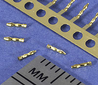
Ziericks wave socket consists of a cone-shaped self-adjusting section, and a pair of progressive wave spring contacts that are attached to the funnel section. When it is inserted into different diameter holes and a contact pin is forced through the sockets, the socket is held in place in the plated-through hole by the self-adjusting compliant press-fit funnel section. It replaces soldered joints in multi-stacked board assemblies and allows an increase in contact density from 2,000 to 7,000 multilayer board connects.
The wave socket is produced in a 30-ton Bruderer press at 450 spm in a two-stage process. The part is blanked in the first die and then formed in a second die. The part is gold plated between steps.
To utilize this product, the printed circuit boards are stacked with metal shielding blocks between them. The wave sockets are inserted into the circuit board holes, with an automatic socket insertion machine. After all boards are completely populated with components, they are stacked in parallel using the spacer shielding blocks between boards to line up the assembly. The assembly is then fastened in place and an automatic pin insertion machine pushes the connecting pins through the sockets boards and shielding blocks.
This product was developed for a customer who needed to stack several dozen multi-layer circuit boards, to produce a three-dimensional circuit board sandwich. The socket allowed the multi-board assemblies to be taken apart and reassembled when repairs were necessary, resulting in a savings of $1,000,000 per year for the customer.
A wide range of critical requirements had to be met with this design. In addition to demanding electrical characteristics, the socket had to work with small (0.020) plated-through holes having large variations in diameter (25 percent). The socket also had to accommodate large hole location tolerances, and could not damage the hole walls. High current-carrying capacity was required and all thermal management requirements had to be satisfied.
Critical requirements included a maximum defect level of 6 ppm. One piece of equipment employed more than 1,000,000 connections, more than 10,000 per board. Life requirement for the sockets was 100 connect/ disconnect cycles.
The solderless interconnection system uses miniature pins that fit into the wave sockets, permitting the stacking of multi-layer circuit boards with plated through-holes varying from 0.020 to 0.025 in diameter to provide a density of 180 signal lines per square inch. The objective of the interconnection system design is to provide a high-speed, high-density matched impedance interface between stacked circuit boards with the shortest signal path.
Zierick Manufacturing Corporation, Mt. Kisco, NY, won the PMA-Higgins Design award for this innovative printed circuit board wave socket. |
|


 Through Hole